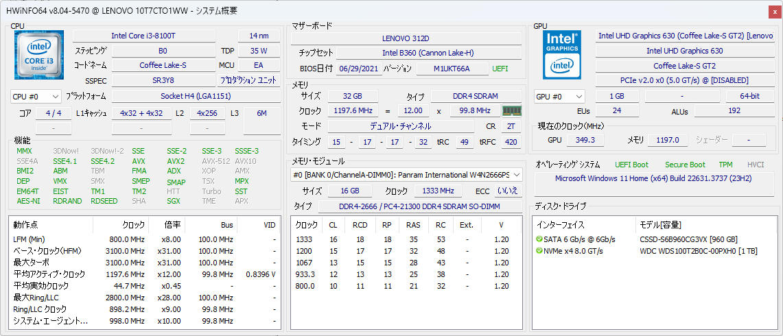
2019年8月末に購入したLenovo ThinkCentre M720qのメモリーを交換し、16GBytesから32GBytesに増量した。
メモリー増量の履歴
| 時期 | 価格 | |
|---|---|---|
| 2024/06 | 16GB×2=32GB | (2枚セット) 9,780円 |
| 2019/12 | 8GB×2=16GB | 3,645円×2=7,290円 |
| 2019/08 | ThinkCentre M720q 新規購入時 4GB×2=8GB | (PC本体) 59,514円 |
ついでに、過去のメモリー交換記録から価格推移の表も貼り付けておく。
| 時期 | 価格 | 容量と取り付けたマシン |
|---|---|---|
| 2024/06 | 4,980円 | DDR4-2666, 16GB×2枚, ThinkCentre M720q |
| 2024/06 | 4,980円 | DDR4-2666, 16GB×1枚, 富士通 LIFEBOOK U938/T |
| 2022/06 | 3,673円 | DDR3-1600, 8GB×2枚, HP EliteDesk 800 G1 DM |
| 2021/09 | 6,425円 | DDR3L-1600, 8GB×2枚, 東芝 dynabook R63/U |
| 2019/12 | 7,290円 | DDR4-2666, 8GB×2枚, Lenovo ThinkCentre M720q |
| 2015/07 | 11,920円 | DDR3-1600, 4GB×4枚(実際2枚), HP s5350 |
| 2009/12 | 29,600円 | DDR2-800, 2GB×8枚(実際1枚), Dell Inspiron mini 10v |
2枚セット品のほうが少し安い
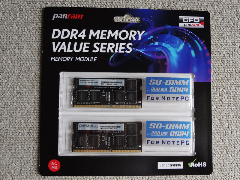
Amazonで、PC4-21300 (DDR4-2666) 16GBytes×2枚セット品を9,780円で購入した。このメモリーは単体で4,980円で売られているものと同一で、セットになると180円ほど安くなっている。
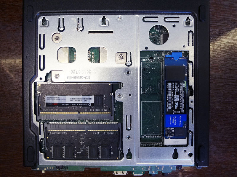
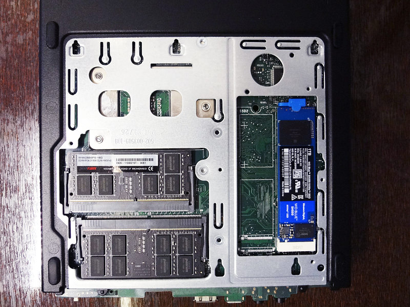
交換作業
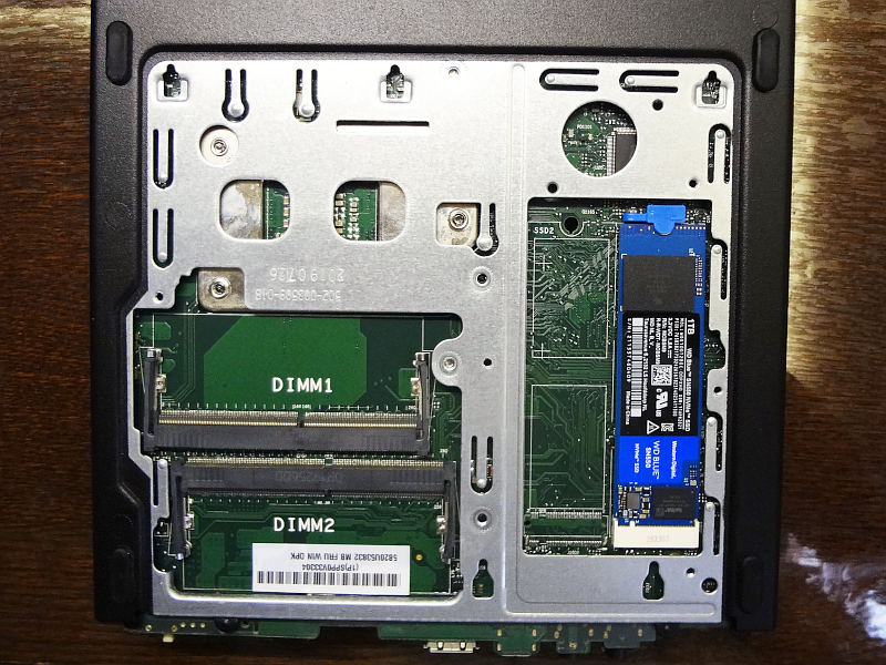
ThinkCentre M720qのメモリーソケット(DDR4 SO-DIMM 260pin)
UEFI BIOSでのメモリーテスト
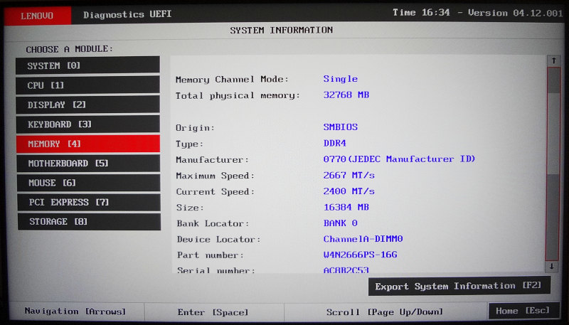
この画面では「Single Channel」で認識されている。Windows起動後のHWiNFOではDual Channelと表示されるので、起動時の何処かの時点でアクセス方式が変更になるのだろう。
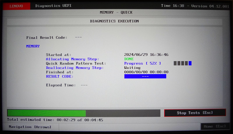
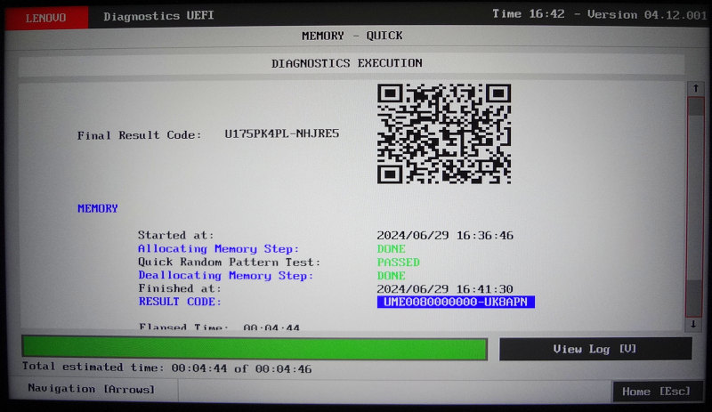
約4分でテストが終了し、「Quick Random Pattern Test : PASSED」と表示された。
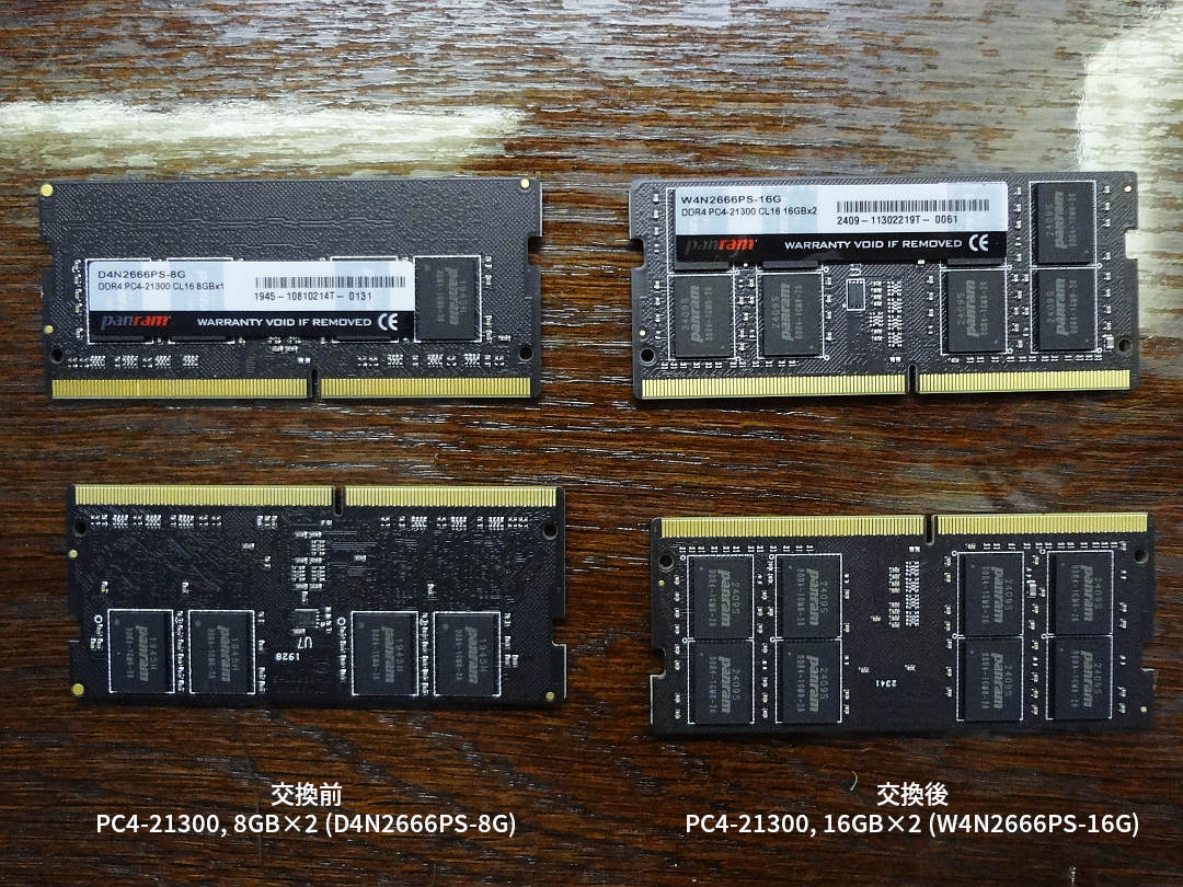
交換前のメモリーを調査
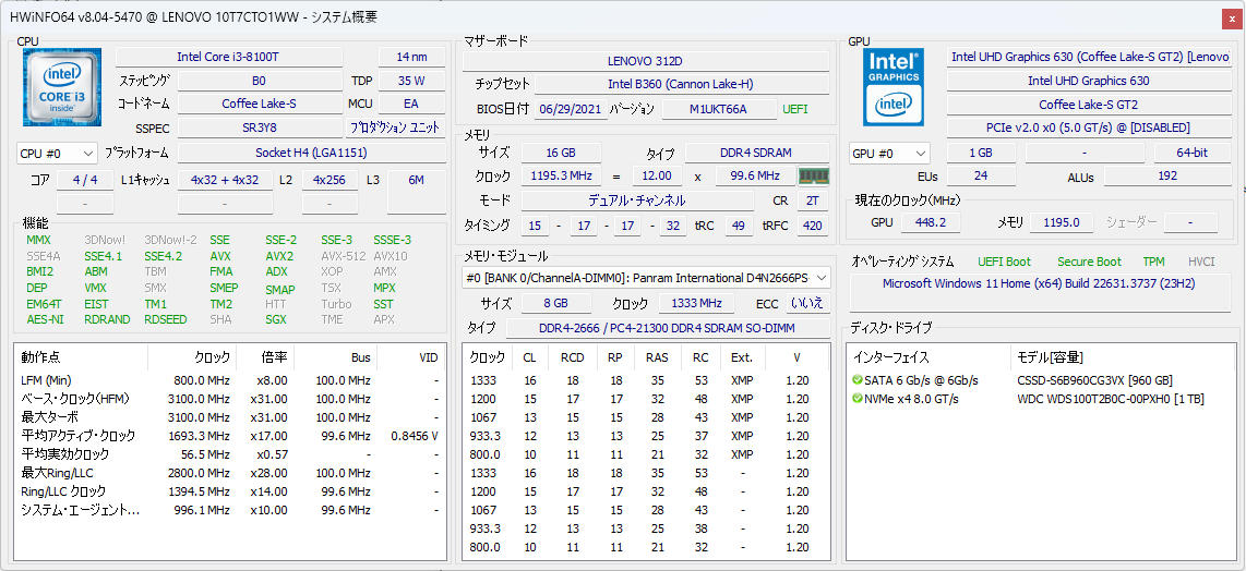
HWiNFOで交換前のメモリー(8GB×2)を調査
HWiNFO64 Version 8.04-5470

WINDOWS11M720Q ------------------------------------------------------------

 [Current Computer]
 [Operating System]

Memory --------------------------------------------------------------------

 [General Information]
  Total Memory Size:                      16 GBytes
  Total Memory Size [MB]:                 16384
 [Current Performance Settings]
  Maximum Supported Memory Clock:         1200.0 MHz
  Current Memory Clock:                   1197.0 MHz
  Current Timing (tCAS-tRCD-tRP-tRAS):    15-17-17-32
  Memory Channels Supported:              2
  Memory Channels Active:                 2
  Command Rate (CR):                      2T
  Read to Read Delay (tRDRD_SG/TrdrdScL) Same Bank Group: 6T
  Read to Read Delay (tRDRD_DG/TrdrdScDlr) Different Bank Group: 4T
  Read to Read Delay (tRDRD_SD) Same DIMM: 6T
  Read to Read Delay (tRDRD_DD) Different DIMM: 7T
  Write to Write Delay (tWRWR_SG/TwrwrScL) Same Bank Group: 6T
  Write to Write Delay (tWRWR_DG/TwrwrScDlr) Different Bank Group: 4T
  Write to Write Delay (tWRWR_SD) Same DIMM: 7T
  Write to Write Delay (tWRWR_DD) Different DIMM: 7T
  Read to Write Delay (tRDWR_SG/TrdwrScL) Same Bank Group: 9T
  Read to Write Delay (tRDWR_DG/TrdwrScDlr) Different Bank Group: 9T
  Read to Write Delay (tRDWR_SD) Same DIMM: 10T
  Read to Write Delay (tRDWR_DD) Different DIMM: 11T
  Write to Read Delay (tWRRD_SG/TwrrdScL) Same Bank Group: 28T
  Write to Read Delay (tWRRD_DG/TwrrdScDlr) Different Bank Group: 22T
  Write to Read Delay (tWRRD_SD) Same DIMM: 6T
  Write to Read Delay (tWRRD_DD) Different DIMM: 6T
  Read to Precharge Delay (tRTP):         9T
  Write to Precharge Delay (tWTP):        30T
  Write Recovery Time (tWR):              19T
  RAS# to RAS# Delay (tRRD_L):            24T
  RAS# to RAS# Delay (tRRD_S):            18T
  Row Cycle Time (tRC):                   49T
  Refresh Cycle Time (tRFC):              420T
  Four Activate Window (tFAW):            26T

Row: 0 [BANK 0/ChannelA-DIMM0] - 8 GB PC4-21300 DDR4 SDRAM Panram International D4N2666PS-8G

 [General Module Information]
  Module Number:                          0
  Module Size:                            8 GBytes
  Memory Type:                            DDR4 SDRAM
  Module Type:                            SO-DIMM
  Memory Speed:                           1333.3 MHz (DDR4-2666 / PC4-21300)
  Module Manufacturer:                    Panram International
  Module Part Number:                     D4N2666PS-8G
  Module Revision:                        0.0
  Module Serial Number:                   1392727633 (51560353)
  Module Manufacturing Date:              Year: 2019, Week: 45
  Module Manufacturing Location:          0
  SDRAM Manufacturer:                     SK Hynix
  DRAM Steppping:                         0.0
  Error Check/Correction:                 None
 [Module Characteristics]
  Row Address Bits:                       16
  Column Address Bits:                    10
  Module Density:                         8192 Mb
  Number Of Ranks:                        1
  Number Of Bank Groups:                  4
  Device Width:                           8 bits
  Bus Width:                              64 bits
  Die Count:                              1
  Module Nominal Voltage (VDD):           1.2 V
  Minimum SDRAM Cycle Time (tCKAVGmin):   0.75000 ns (1333 MHz)
  Maximum SDRAM Cycle Time (tCKAVGmax):   1.62500 ns
  CAS# Latencies Supported:               9, 10, 11, 12, 13, 14, 15, 16, 17, 18, 19, 20
  Minimum CAS# Latency Time (tAAmin):     12.000 ns
  Minimum RAS# to CAS# Delay (tRCDmin):   13.500 ns
  Minimum Row Precharge Time (tRPmin):    13.500 ns
  Minimum Active to Precharge Time (tRASmin): 26.125 ns
  Supported Module Timing at 1333.3 MHz:  16-18-18-35
  Supported Module Timing at 1200.0 MHz:  15-17-17-32
  Supported Module Timing at 1066.7 MHz:  13-15-15-28
  Supported Module Timing at 933.3 MHz:   12-13-13-25
  Supported Module Timing at 800.0 MHz:   10-11-11-21
  Minimum Active to Active/Refresh Time (tRCmin): 39.750 ns
  Minimum Refresh Recovery Time Delay (tRFC1min): 350.000 ns
  Minimum Refresh Recovery Time Delay (tRFC2min): 260.000 ns
  Minimum Refresh Recovery Time Delay (tRFC4min): 160.000 ns
  Minimum Four Activate Window Delay Time (tFAWmin): 21.000 ns
  Minimum Active to Active Delay Time - Different Bank Group (tRRD_Smin): 3.674 ns
  Minimum Active to Active Delay Time - Same Bank Group (tRRD_Lmin): 5.900 ns
  Minimum CAS to CAS Delay Time - Same Bank Group (tCCD_Lmin): 5.250 ns
 [Features]
  Module Temperature Sensor (TSOD):       Not Supported
  Module Nominal Height:                  29 - 30 mm
  Module Maximum Thickness (Front):       1 - 2 mm
  Module Maximum Thickness (Back):        1 - 2 mm
  Address Mapping from Edge Connector to DRAM: Mirrored
 [Intel Extreme Memory Profile (XMP)]
  XMP Revision:                           2.0
 [Certified Profile [Enabled]]
  Module VDD Voltage Level:               1.20 V
  Minimum SDRAM Cycle Time (tCKAVGmin):   0.75000 ns (1333 MHz)
  CAS# Latencies Supported:               9, 10, 11, 12, 13, 14, 15, 16, 17, 18, 19, 20
  Minimum CAS# Latency Time (tAAmin):     11.875 ns
  Minimum RAS# to CAS# Delay (tRCDmin):   13.375 ns
  Minimum Row Precharge Time (tRPmin):    13.375 ns
  Minimum Active to Precharge Time (tRASmin): 26.125 ns
  Supported Module Timing at 1333.3 MHz:  16-18-18-35
  Supported Module Timing at 1200.0 MHz:  15-17-17-32
  Supported Module Timing at 1066.7 MHz:  13-15-15-28
  Supported Module Timing at 933.3 MHz:   12-13-13-25
  Supported Module Timing at 800.0 MHz:   10-11-11-21
  Minimum Active to Active/Refresh Time (tRCmin): 39.500 ns
  Minimum Refresh Recovery Time Delay (tRFC1min): 350.000 ns
  Minimum Refresh Recovery Time Delay (tRFC2min): 260.000 ns
  Minimum Refresh Recovery Time Delay (tRFC4min): 160.000 ns
  Minimum Four Activate Window Delay Time (tFAWmin): 25.000 ns
  Minimum Active to Active Delay Time - Different Bank Group (tRRD_Smin): 4.299 ns
  Minimum Active to Active Delay Time - Same Bank Group (tRRD_Lmin): 6.525 ns

Row: 2 [BANK 2/ChannelB-DIMM0] - 8 GB PC4-21300 DDR4 SDRAM Panram International D4N2666PS-8G

 [General Module Information]
  Module Number:                          2
  Module Size:                            8 GBytes
  Memory Type:                            DDR4 SDRAM
  Module Type:                            SO-DIMM
  Memory Speed:                           1333.3 MHz (DDR4-2666 / PC4-21300)
  Module Manufacturer:                    Panram International
  Module Part Number:                     D4N2666PS-8G
  Module Revision:                        0.0
  Module Serial Number:                   1392726954 (AA530353)
  Module Manufacturing Date:              Year: 2019, Week: 45
  Module Manufacturing Location:          0
  SDRAM Manufacturer:                     SK Hynix
  DRAM Steppping:                         0.0
  Error Check/Correction:                 None
 [Module Characteristics]
  Row Address Bits:                       16
  Column Address Bits:                    10
  Module Density:                         8192 Mb
  Number Of Ranks:                        1
  Number Of Bank Groups:                  4
  Device Width:                           8 bits
  Bus Width:                              64 bits
  Die Count:                              1
  Module Nominal Voltage (VDD):           1.2 V
  Minimum SDRAM Cycle Time (tCKAVGmin):   0.75000 ns (1333 MHz)
  Maximum SDRAM Cycle Time (tCKAVGmax):   1.62500 ns
  CAS# Latencies Supported:               9, 10, 11, 12, 13, 14, 15, 16, 17, 18, 19, 20
  Minimum CAS# Latency Time (tAAmin):     12.000 ns
  Minimum RAS# to CAS# Delay (tRCDmin):   13.500 ns
  Minimum Row Precharge Time (tRPmin):    13.500 ns
  Minimum Active to Precharge Time (tRASmin): 26.125 ns
  Supported Module Timing at 1333.3 MHz:  16-18-18-35
  Supported Module Timing at 1200.0 MHz:  15-17-17-32
  Supported Module Timing at 1066.7 MHz:  13-15-15-28
  Supported Module Timing at 933.3 MHz:   12-13-13-25
  Supported Module Timing at 800.0 MHz:   10-11-11-21
  Minimum Active to Active/Refresh Time (tRCmin): 39.750 ns
  Minimum Refresh Recovery Time Delay (tRFC1min): 350.000 ns
  Minimum Refresh Recovery Time Delay (tRFC2min): 260.000 ns
  Minimum Refresh Recovery Time Delay (tRFC4min): 160.000 ns
  Minimum Four Activate Window Delay Time (tFAWmin): 21.000 ns
  Minimum Active to Active Delay Time - Different Bank Group (tRRD_Smin): 3.674 ns
  Minimum Active to Active Delay Time - Same Bank Group (tRRD_Lmin): 5.900 ns
  Minimum CAS to CAS Delay Time - Same Bank Group (tCCD_Lmin): 5.250 ns
 [Features]
  Module Temperature Sensor (TSOD):       Not Supported
  Module Nominal Height:                  29 - 30 mm
  Module Maximum Thickness (Front):       1 - 2 mm
  Module Maximum Thickness (Back):        1 - 2 mm
  Address Mapping from Edge Connector to DRAM: Mirrored
 [Intel Extreme Memory Profile (XMP)]
  XMP Revision:                           2.0
 [Certified Profile [Enabled]]
  Module VDD Voltage Level:               1.20 V
  Minimum SDRAM Cycle Time (tCKAVGmin):   0.75000 ns (1333 MHz)
  CAS# Latencies Supported:               9, 10, 11, 12, 13, 14, 15, 16, 17, 18, 19, 20
  Minimum CAS# Latency Time (tAAmin):     11.875 ns
  Minimum RAS# to CAS# Delay (tRCDmin):   13.375 ns
  Minimum Row Precharge Time (tRPmin):    13.375 ns
  Minimum Active to Precharge Time (tRASmin): 26.125 ns
  Supported Module Timing at 1333.3 MHz:  16-18-18-35
  Supported Module Timing at 1200.0 MHz:  15-17-17-32
  Supported Module Timing at 1066.7 MHz:  13-15-15-28
  Supported Module Timing at 933.3 MHz:   12-13-13-25
  Supported Module Timing at 800.0 MHz:   10-11-11-21
  Minimum Active to Active/Refresh Time (tRCmin): 39.500 ns
  Minimum Refresh Recovery Time Delay (tRFC1min): 350.000 ns
  Minimum Refresh Recovery Time Delay (tRFC2min): 260.000 ns
  Minimum Refresh Recovery Time Delay (tRFC4min): 160.000 ns
  Minimum Four Activate Window Delay Time (tFAWmin): 25.000 ns
  Minimum Active to Active Delay Time - Different Bank Group (tRRD_Smin): 4.299 ns
  Minimum Active to Active Delay Time - Same Bank Group (tRRD_Lmin): 6.525 ns
交換後のメモリーを調査
HWiNFOで交換前のメモリー(8GB×2)を調査
HWiNFO64 Version 8.04-5470

WINDOWS11M720Q ------------------------------------------------------------

 [Current Computer]
 [Operating System]

Memory --------------------------------------------------------------------

 [General Information]
  Total Memory Size:                      32 GBytes
  Total Memory Size [MB]:                 32768
 [Current Performance Settings]
  Maximum Supported Memory Clock:         1200.0 MHz
  Current Memory Clock:                   1197.5 MHz
  Current Timing (tCAS-tRCD-tRP-tRAS):    15-17-17-32
  Memory Channels Supported:              2
  Memory Channels Active:                 2
  Command Rate (CR):                      2T
  Read to Read Delay (tRDRD_SG/TrdrdScL) Same Bank Group: 6T
  Read to Read Delay (tRDRD_DG/TrdrdScDlr) Different Bank Group: 4T
  Read to Read Delay (tRDRD_SD) Same DIMM: 6T
  Read to Read Delay (tRDRD_DD) Different DIMM: 7T
  Write to Write Delay (tWRWR_SG/TwrwrScL) Same Bank Group: 6T
  Write to Write Delay (tWRWR_DG/TwrwrScDlr) Different Bank Group: 4T
  Write to Write Delay (tWRWR_SD) Same DIMM: 7T
  Write to Write Delay (tWRWR_DD) Different DIMM: 7T
  Read to Write Delay (tRDWR_SG/TrdwrScL) Same Bank Group: 9T
  Read to Write Delay (tRDWR_DG/TrdwrScDlr) Different Bank Group: 9T
  Read to Write Delay (tRDWR_SD) Same DIMM: 9T
  Read to Write Delay (tRDWR_DD) Different DIMM: 11T
  Write to Read Delay (tWRRD_SG/TwrrdScL) Same Bank Group: 28T
  Write to Read Delay (tWRRD_DG/TwrrdScDlr) Different Bank Group: 22T
  Write to Read Delay (tWRRD_SD) Same DIMM: 5T
  Write to Read Delay (tWRRD_DD) Different DIMM: 6T
  Read to Precharge Delay (tRTP):         9T
  Write to Precharge Delay (tWTP):        30T
  Write Recovery Time (tWR):              19T
  RAS# to RAS# Delay (tRRD_L):            24T
  RAS# to RAS# Delay (tRRD_S):            18T
  Row Cycle Time (tRC):                   49T
  Refresh Cycle Time (tRFC):              420T
  Four Activate Window (tFAW):            26T

Row: 0 [BANK 0/ChannelA-DIMM0] - 16 GB PC4-21300 DDR4 SDRAM Panram International W4N2666PS-16G

 [General Module Information]
  Module Number:                          0
  Module Size:                            16 GBytes
  Memory Type:                            DDR4 SDRAM
  Module Type:                            SO-DIMM
  Memory Speed:                           1333.3 MHz (DDR4-2666 / PC4-21300)
  Module Manufacturer:                    Panram International
  Module Part Number:                     W4N2666PS-16G
  Module Revision:                        0.0
  Module Serial Number:                   1395428268 (AC8B2C53)
  Module Manufacturing Date:              Year: 2024, Week: 9
  Module Manufacturing Location:          0
  SDRAM Manufacturer:                     Samsung
  DRAM Steppping:                         0.0
  Error Check/Correction:                 None
 [Module Characteristics]
  Row Address Bits:                       16
  Column Address Bits:                    10
  Module Density:                         8192 Mb
  Number Of Ranks:                        2
  Number Of Bank Groups:                  4
  Device Width:                           8 bits
  Bus Width:                              64 bits
  Die Count:                              1
  Module Nominal Voltage (VDD):           1.2 V
  Minimum SDRAM Cycle Time (tCKAVGmin):   0.75000 ns (1333 MHz)
  Maximum SDRAM Cycle Time (tCKAVGmax):   1.62500 ns
  CAS# Latencies Supported:               9, 10, 11, 12, 13, 14, 15, 16, 17, 18, 19, 20
  Minimum CAS# Latency Time (tAAmin):     12.000 ns
  Minimum RAS# to CAS# Delay (tRCDmin):   13.500 ns
  Minimum Row Precharge Time (tRPmin):    13.500 ns
  Minimum Active to Precharge Time (tRASmin): 26.125 ns
  Supported Module Timing at 1333.3 MHz:  16-18-18-35
  Supported Module Timing at 1200.0 MHz:  15-17-17-32
  Supported Module Timing at 1066.7 MHz:  13-15-15-28
  Supported Module Timing at 933.3 MHz:   12-13-13-25
  Supported Module Timing at 800.0 MHz:   10-11-11-21
  Minimum Active to Active/Refresh Time (tRCmin): 39.750 ns
  Minimum Refresh Recovery Time Delay (tRFC1min): 350.000 ns
  Minimum Refresh Recovery Time Delay (tRFC2min): 260.000 ns
  Minimum Refresh Recovery Time Delay (tRFC4min): 160.000 ns
  Minimum Four Activate Window Delay Time (tFAWmin): 21.000 ns
  Minimum Active to Active Delay Time - Different Bank Group (tRRD_Smin): 3.674 ns
  Minimum Active to Active Delay Time - Same Bank Group (tRRD_Lmin): 5.900 ns
  Minimum CAS to CAS Delay Time - Same Bank Group (tCCD_Lmin): 5.250 ns
 [Features]
  Module Temperature Sensor (TSOD):       Not Supported
  Module Nominal Height:                  29 - 30 mm
  Module Maximum Thickness (Front):       1 - 2 mm
  Module Maximum Thickness (Back):        1 - 2 mm
  Address Mapping from Edge Connector to DRAM: Mirrored

Row: 2 [BANK 2/ChannelB-DIMM0] - 16 GB PC4-21300 DDR4 SDRAM Panram International W4N2666PS-16G

 [General Module Information]
  Module Number:                          2
  Module Size:                            16 GBytes
  Memory Type:                            DDR4 SDRAM
  Module Type:                            SO-DIMM
  Memory Speed:                           1333.3 MHz (DDR4-2666 / PC4-21300)
  Module Manufacturer:                    Panram International
  Module Part Number:                     W4N2666PS-16G
  Module Revision:                        0.0
  Module Serial Number:                   1395428648 (288D2C53)
  Module Manufacturing Date:              Year: 2024, Week: 9
  Module Manufacturing Location:          0
  SDRAM Manufacturer:                     Samsung
  DRAM Steppping:                         0.0
  Error Check/Correction:                 None
 [Module Characteristics]
  Row Address Bits:                       16
  Column Address Bits:                    10
  Module Density:                         8192 Mb
  Number Of Ranks:                        2
  Number Of Bank Groups:                  4
  Device Width:                           8 bits
  Bus Width:                              64 bits
  Die Count:                              1
  Module Nominal Voltage (VDD):           1.2 V
  Minimum SDRAM Cycle Time (tCKAVGmin):   0.75000 ns (1333 MHz)
  Maximum SDRAM Cycle Time (tCKAVGmax):   1.62500 ns
  CAS# Latencies Supported:               9, 10, 11, 12, 13, 14, 15, 16, 17, 18, 19, 20
  Minimum CAS# Latency Time (tAAmin):     12.000 ns
  Minimum RAS# to CAS# Delay (tRCDmin):   13.500 ns
  Minimum Row Precharge Time (tRPmin):    13.500 ns
  Minimum Active to Precharge Time (tRASmin): 26.125 ns
  Supported Module Timing at 1333.3 MHz:  16-18-18-35
  Supported Module Timing at 1200.0 MHz:  15-17-17-32
  Supported Module Timing at 1066.7 MHz:  13-15-15-28
  Supported Module Timing at 933.3 MHz:   12-13-13-25
  Supported Module Timing at 800.0 MHz:   10-11-11-21
  Minimum Active to Active/Refresh Time (tRCmin): 39.750 ns
  Minimum Refresh Recovery Time Delay (tRFC1min): 350.000 ns
  Minimum Refresh Recovery Time Delay (tRFC2min): 260.000 ns
  Minimum Refresh Recovery Time Delay (tRFC4min): 160.000 ns
  Minimum Four Activate Window Delay Time (tFAWmin): 21.000 ns
  Minimum Active to Active Delay Time - Different Bank Group (tRRD_Smin): 3.674 ns
  Minimum Active to Active Delay Time - Same Bank Group (tRRD_Lmin): 5.900 ns
  Minimum CAS to CAS Delay Time - Same Bank Group (tCCD_Lmin): 5.250 ns
 [Features]
  Module Temperature Sensor (TSOD):       Not Supported
  Module Nominal Height:                  29 - 30 mm
  Module Maximum Thickness (Front):       1 - 2 mm
  Module Maximum Thickness (Back):        1 - 2 mm
  Address Mapping from Edge Connector to DRAM: Mirrored

